Advanced Power Semiconductor Laboratory (APS)
The Advanced Power Semiconductor (APS) Laboratory at the Department of Information Technology and Electrical Engineering of the ETH Zurich is building up a strong competence in novel power semiconductor devices based on wide band-gap (WBG) materials that represent the core of today’s energy efficient power electronics.
As part of ETH Zurich‘s Energy Initiative, the APS Laboratory was founded in 2015. Prof. Dr. Ulrike Grossner, the head of the APS Laboratory, has established a research center and an educational platform at ETH for the design, optimization, and manufacturing of novel power electronics devices and their modules.
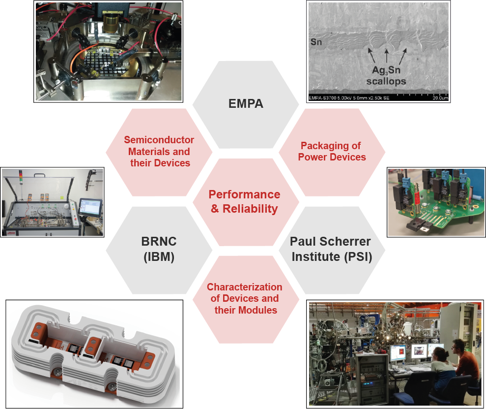
Today’s requirements for higher levels of integration, higher operating temperatures, and higher blocking voltages rise the demand for advanced power electronic systems based on WBG power semiconductors. New generation of power semiconductors rely substantially on material science and new processing technologies. Automotive industry, solar power systems, more electric aircraft, and naval industry are some of the energy applications that foster the current technology innovations in the power semiconductors domain. The ongoing research within the APS covers the multi-disciplinary topics, including 2D/3D modelling and simulation of power semiconductors and their packaging, the fabrication of semiconductor devices, and new technologies for the advanced high performance power modules. In collaboration with EMPA and PSI, the APS team works towards innovative solutions for full utilization of silicon carbide, utilizing its advantages over silicon in reliable power electronic systems. The fabrication of power devices will be performed in the cleanroom of BRNC located at IBM Zurich.
